06 Datapath
MIPS Datapath
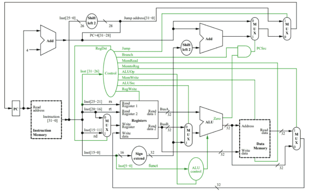
Goal of Datapath
Build an architecture to support the following instructions
- Arithmetic:
add,sub,addi,slt - Memory references:
lw,sw - Branches:
j,beq
Process
- Design basic framework that is needed by all instructions
- Build a computer for each operation individually
- Add MUXs to choose between different operations
- Add control signals to control the MUXs
MIPS Steps
flowchart LR
if["Instruction Fetch<br/>(using Program Counter)"] -->
|PC += 4| r["Instruction Decode<br />&<br />Register Read"] -->
alu["Execute<br />(ALU)"] -->
m["Memory<br />(Read/Write)"] -->
R["WriteBack<br />(Register Write)"]
Register Read may be
- One register:
addi,lw - Two registers:
add,sub,slt,sw,beq
Quick operations may loop twice through machine, getting incorrect result, as clock is dependent on longest path (lw).
Sign Extension
Important for immediate data operations
Take the top bit and copy it to all the other bits
example
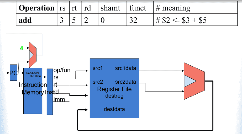
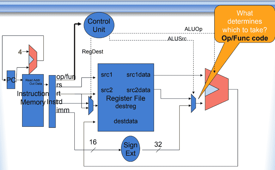
MIPS Instruction Available Datapath
add instruction
addi Instruction
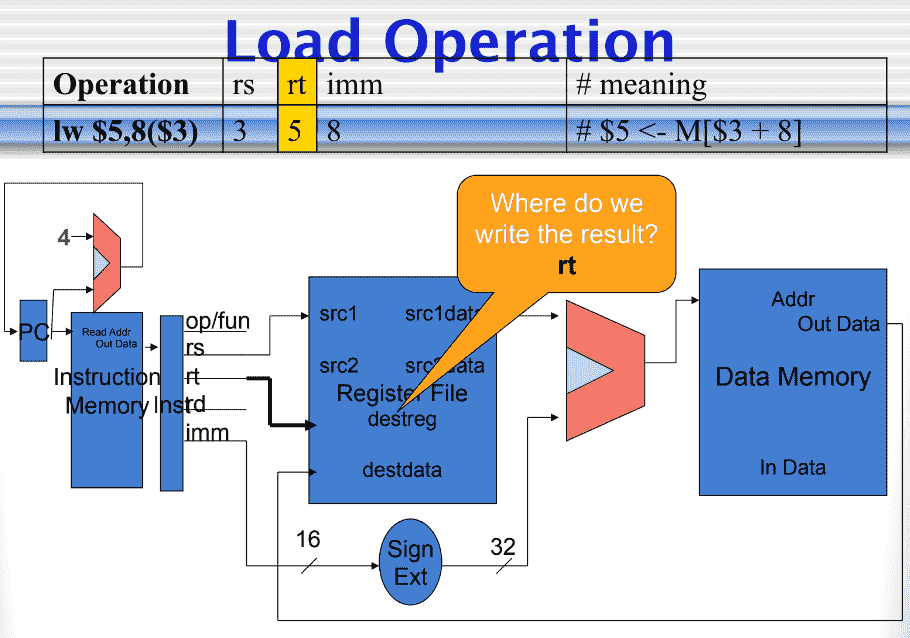
load Instruction
Store Instruction
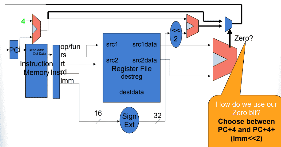
beq Instruction
Choose between
- \(\text{PC = (PC + 4)}\)
- \(\text{PC = (PC + 4) + \ \ Imm<<2}\)
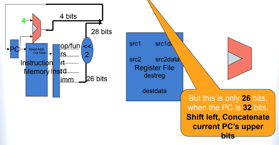
j Instruction
imm is 26 bits, but PC is 32 bits
imm <<(shift left)- Concatenate PC’s upper bits
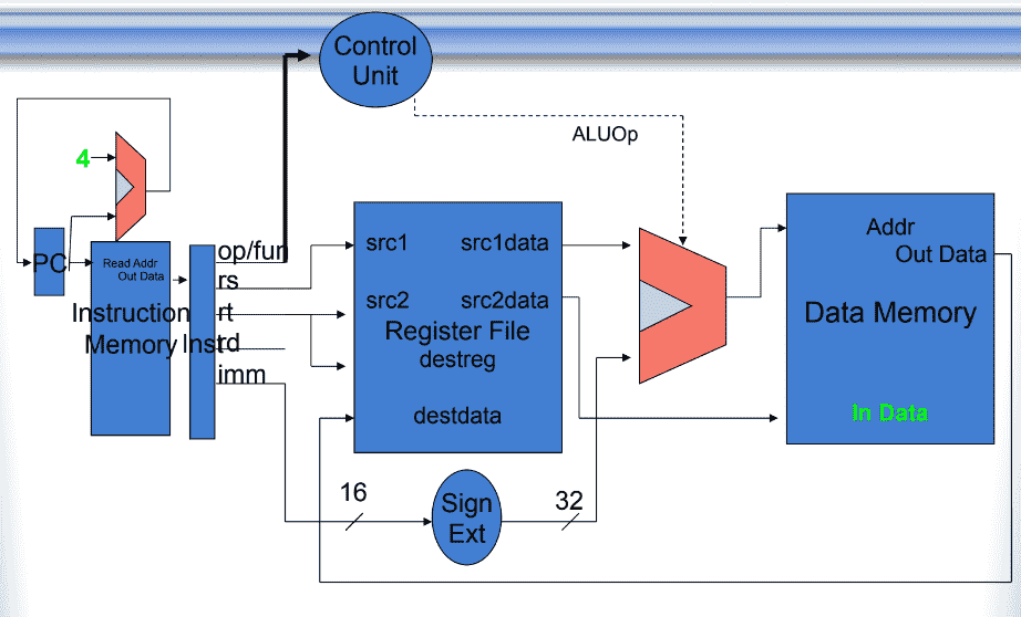
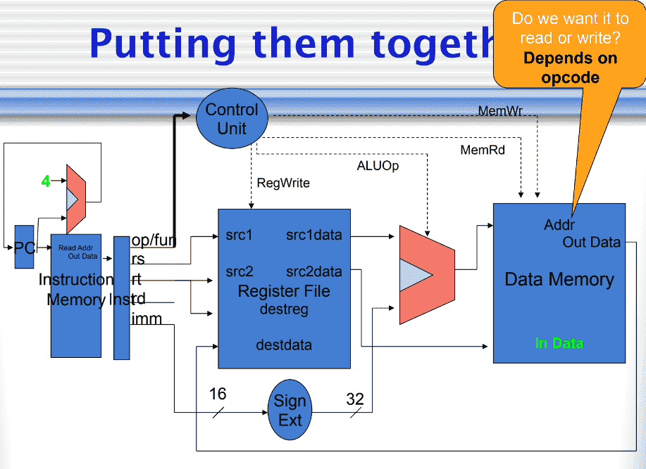
Control Unit
Set of control line values that cause appropriate actions to be taken at each step
Finite state machine determines what needs to be done at each step
- Fetch
- Decode
- Action depends on opcode
- Execute
- Memory
- Writeback
Single Cycle implementation
An implementation in which an instruction is executed in one clock cycle
Also called single clock cycle implementation
Advantage
Easy to understand
Disadvantage
Too slow
The clock cycle must have the same length for every instruction. Hence, the longest possible path in the processor determines the clock cycle
- usually it is the
loadinstruction, which uses five functional units in series- instruction memory
- register file
- ALU
- data memory
- register file
Single long clock cycle makes add take as long as load
Solution
- Break single instruction execution into small execution steps
- Improve performance by pipelining